Cliff Orori Mosiori
Abstract: Hybrid perovskite solar cells have been developing at a staggering pace in just a few years with the first perovskite cell reported in 2009 managing about 4% PCE. By 2015, perovskite cells had been certified as having more than 20-percent efficiency. However, a number of questions on methyl ammonium lead trihalide (CH3NH3PbI3) absorbers remain unanswered. This includes its varying PCE values obtained through rapid reverse and forward scans that yield anomalous hysterical efficiencies. Already, NREL certified PCE values of CH3NH3PbI3 solar cell is classified as “unreliable” and not be justifiable for patenting. Solar efficiency basically relies on the behavior of I-V characteristic curve. Such revelations require consistent experimental investigations to explain how electron or charge mobility traverses through CH3NH3PbI3 thin films through consistent reproducible experimental techniques like the solvent-solvent extraction method. Photoluminescence measurements; Atomic Force Microscopy, cross-sectional scanning transmission electron microscopy and Time-of-Flight spectrometry are important paramount investigations that can reveal amazing intrinsic relations to electron mobility and transport mechanisms especially those carried with temperature dependent longitudinal and Hall resistances measurements using the standard four-terminal method.
Keywords: Photoluminescence; Time-of-Flight spectrometry, perovskite solar cell, PCE efficiencies.
- INTRODUCTION:
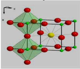
Researchers have come up with a number of new techniques of fabricating perovskite films for solid state applications. Some techniques are well suited for making ultra-thin films that are semi-transparent having a capability of making solar cells of different colors. Perovskites are a class of crystalline materials with excellent light absorption levels and much cheaper to make than the silicon wafers. The crystal structure of CH3NH3PbI3 has its CH3NH3+ surrounded by PbI6 octahedra [13] making CH3NH3PbI3 to be classified as a perovskite material. Its crystal structure is shown in Figure 1. When such materials are used in solar technology as absorbers, they result into perovskite solar cells and the presence of lead in CH3NH3PbI3 makes it a hybrid solar cell. Therefore a perovskite solar cell employs a perovskite structured material as its absorber layer [38]. Thin films of CH3NH3PbI3 have a band gap between 1.5 – 2.3 eV depending on its iodide concentration [14] which is a band gap close to an optimal gap for single-junction cells [47, 41]. They also have very strong photon absorption levels [67, 75] in the visible region.
Already, prototype solar cells have achieved PCE efficiencies ranging from 3.8% [33] in 2009 to 21.0% [9, 58] in 2015. However, by February 2016, the major hurdle that was facing CH3NH3PbI3 perovskite solar cell was that their PCE values determined through rapid reverse and forward I-V scans was yielding anomalous hysteric efficiencies. It’s generally accepted that the concept behind rapid reverse and forward I-V scans is electron mobility or transfer. Electron transfer is the simplest chemical reaction known in which an electron is transferred from a donor to an acceptor or from a molecular donor state into a particular molecular acceptor state [10] without breaking or creating a chemical bond. It’s also generally accepted that the working principles of a solar cell can be explained based on the concept of electron mobility across its junction [22] in which the solar cell’s response to electron mobility depends on the density of the electrons or carriers involved, their effective mass [61] and their distribution [35]. However, in CH3NH3PbI3 cells, PCE efficiencies are anomalously hysterical, and this suggests that the effect of electron mobility on CH3NH3PbI3 PCE may be different from the above generally acceptable response in inorganic solar cells.
2. INTRINSIC PARAMETERS IN CH3NH3PBI3 SOLAR CELL:
Electron mobility plays an important role on solar cell PCE. The anomalous hysterical efficiencies observed in CH3NH3PbI3 solar cells as a result of rapid I-V reverse bias and forward bias scan [5] has become a challenge to NREL in accepting and patenting PCE especially when the scanning parameters exceed the time-scale required for the CH3NH3PbI3 layer to attain an electronic steady-state [66, 71]. A number of experimental attempts have been made to normalize these scan I-V curves [47] but they have failed and instead increased the risk of producing inflated PCE
Page-1
values [1]. Some experimental analysis on CH3NH3PbI3 solar cells suggest that the likely cause of hysteresis could be due to ion or charge carrier migration or electron mobility [13, 35] without exhaustive describing its effects on hysteresis in PCE of CH3NH3PbI3 Perovskite solar cells.
3. CH3NH3PBI3 THIN FILM RESEARCH:
In February 2016, NREL revealed that CH3NH3PbI3 solar cell based on rapid I-V reverse and forward biased scans were still considered “unreliable” because their PCE efficiencies were anomalously hysterical [20]. This challenge was abided because investigations into the instability of PCE values revealed hysteresis. These investigations proposed that partly, the cause of PCE anomalous hysteresis is due to electron mobility [13, 35] which is a core parameter that determines solar cell efficiency. Questions on how it affects hysteresis started flowing in that required a through investigation for them to be exhaustively understood and explained. Since electron mobility plays a crucial role in solar cell PCE, a thorough investigation to establish the effect of electron mobility on the hysteresis in PCE of CH3NH3PI3 perovskite is of essence. A number of parameters need to be reinvestigated. These include: fluorescence measurements to determine CH3NH3PbI3 exact concentrations resulting in particular hysterical behavior; optical absorption properties per concentration and growth conditions; Faradic currents through CH3NH3PbI3 electrodes using a conventional three-electrode cell to depict electron mobility; electrical and optical transport properties through temperature dependent longitudinal and Hall resistances in a standard four-terminal method. Other proposed investigations include clear and precise elemental compositions measurement using X-ray photoelectron spectroscopy (XPS); determination of apparent free carrier concentration, presence, and location of the confined electrons using Capacitance-Voltage Measurements to unveil scattering centers and photoluminescence measurements at different concentrations, clear valence band structure determinations using ultraviolet photoelectron spectroscopy. Likewise, it has been proposed that computation of time of Flight of an electron in relation to threading dislocations in CH3NH3PbI3 may reveal striking revelations.
- REVIEW OF RELATED STUDIES:
A perovskite solar cell functions in a number of different ways depending on the role of its perovskite absorber layer [78] or the nature of its contact electrodes [13]. Perovskite solar cells whose positive charges are extracted by a transparent bottom electrode are classified as either ‘sensitized cells’ or ‘thin-film cells’ [10]. In ‘sensitized cell’ forms, the perovskite layer is believed to function mainly as a light absorber only [40] while charge mobility occurs in other layers [6]. In ‘thin-film cell’ forms, most of the charge mobility takes place in the bulk perovskite absorber layer itself only [61] and thus, charges are transported through the perovskite layer as light absorption causes charge generation [49]. Perovskite materials were first incorporated into solar cell technology in 2009 [33] using a ‘dye
sensitized solar cell architecture’ achieving 3.8% PCE. In 2011, it achieved 6.5% PCE [28] while a breakthrough was attained in 2012 when a hole transport layer was incorporated [37] resulting into about 10% efficiency. In a ‘sensitized cell form’ with a TiO2 architecture [23, 31, 32], the efficiency was above 10%. Further trials [39] only increased open-circuit voltages. In all these literature, the CH3NH3PbI3 layer was observed to transport holes [24], electrons [5] and excitons [59, 60]. These observations, convinced solar cell research in perovskite solar cell technology to adopted a thin-film approach in 2013 [6]. The resulting impact was a record efficiency greater than 10% [29] and even exceeding 15% [14, 15] in 2013. Techniques for growing CH3NH3PbI3 thin films for solar cells have been evolving. Techniques ranging from thermal evaporation have resulted in solar cells with efficiencies above 15% [11, 25, 39]. More new deposition techniques have been reported in 2014 [8, 17, 18, 21, 34, 50, 51, 54, 57, 63, 68, 74,] corresponding higher PCE. In the mid of 2015 [7, 12, 64, 72] it became apparent that CH3NH3PbI3 solar cells function well in a thin-film architecture as proposed by Xiao et al. [71] and Noel et al.. [47]. In thin-film architecture, it simplified the whole process of determining cell PCE to using rapid reverse and forward biased I-V scans just like in any other inorganic thin film solar cell [27, 55] since normally solar cells PCE is one determined using I-V scans.
Despite all these great achievements, CH3NH3PbI3 solar cells have displayed a unique characteristic behavior. Based on their rapid reverse and forward biased scans, a diverse number of ambiguous PCE values have been reported in literature [16, 31, 32, 45, 56]. As an example, Zhou et al. [76] reported an efficiency of 19.3% while Snath et al. [59, 60] and Unger et al. [66] both reported an efficiency of about 21.0% with ambiguous anomalous hysteretic that depended on scanning conditions (scan direction, scan speed, light soaking and biasing). An analysis on these curves by Ahn et al. [4] revealed a discrepancy between forward-bias to short-circuit and vice versa that evidently showed hysteresis. A few articles acknowledge hysteretic behavior [1, 17, 18, 31, 32, 46, 47, 49, 59, 60, 57, 73, 75] and fewer agree to slow non-hysteretic I-V curves to little or no hysteresis [71] on extremely slow scans which is believed to allow the system to settle into a steady-state condition [20] to eliminate hysteresis. However, these slow scans fail by yielding lower efficiency values when compared to fast I-V-scans. However, extremely slow voltage-scans which eliminate hysteresis may be holding a key to unfold the anomalous hysteric behaviour. Various propositional explanations have been put forth to be investigated which include but they are not limited to ion movement [13], electric polarization [29, 64], ferroelectric effects [8, 17, 18, 34, 68], large-scale trapping of electrons [24] and filling of trap states [66]. Minemoto, and Murata, [43] investigated the impact of the interface in hole/electron transportation and reported its significance in charge mobility while Lang et al. [35] modeled electron transfer using the first principles parameters (e.g., band gap, effective mass etc) and now this work intends to investigate
Page-2
5. MODELING ANALYSIS APPROACHES:
Already CH3NH3PbX3 thin films displays a carrier diffusion length of over one micron [61, 10] enabling its band gap to be tuned by varying its halide concentration [13, 14, 48] in thin film form. However, in its precursor solution, electron behavior can be investigated using its Redox analysis. By applying Nernst Redox reaction equation, its electrochemical potential () can be taken to be equivalent to its Fermi level () as:
